Luke Kenneth Casson Leighton
2017-06-15 14:02:07 UTC
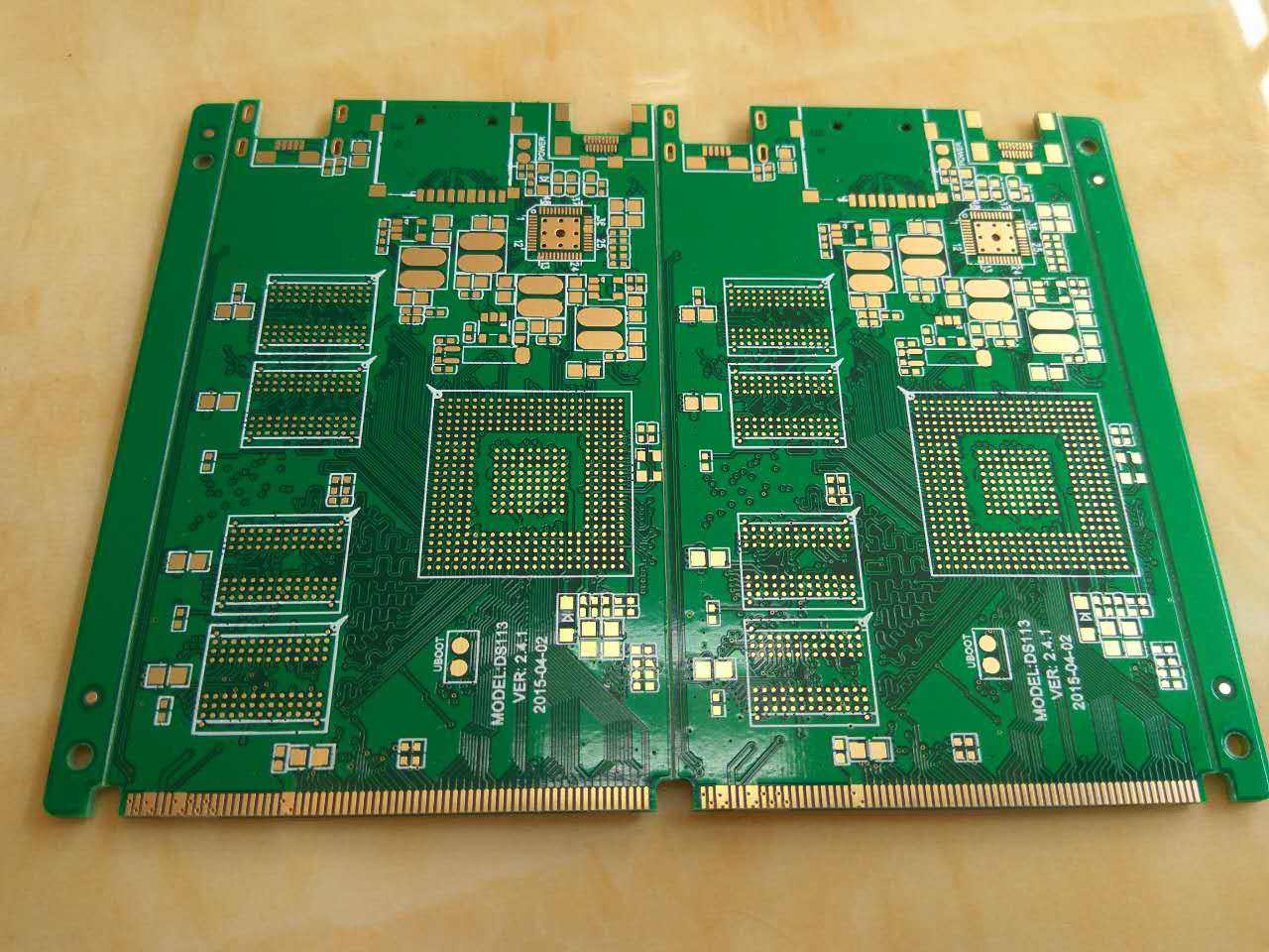
i received the latest pre-production cards yesterday and have tested
one of them: it works.
however (and this is the whole point of doing pre-production
prototypes) in endeavouring to use automated assembly and solder paste
it was discovered that the VIAs underneath the pads for the JAE DC3
Micro-HDMI connector are sucking the solder paste in and down, leaving
the pins not properly connected.
the factory's engineer hand-soldered the 10 samples, but we cannot
possibly do 1,000 PCBs by hand.... so it is necessary to do some test
PCBs to work out how to get these connectors, with utterly tiny pins
(0.25mm wide) to stick, given that the tracks simply have to come up
from underneath using VIAs.
VIAs coming up on a pad is generally bad because it's a hole down
which the solder paste simply... sucks down.
if anyone knows any tricks i would appreciate hearing them. i was
thinking of creating the pad with a triangular end, placing the VIA
right at the end so that the solder paste can't "wick away". anyone
got any other ideas?
l.
---
crowd-funded eco-conscious hardware: https://www.crowdsupply.com/eoma68
_______________________________________________
arm-netbook mailing list arm-***@lists.phcomp.co.uk
http://lists.phcomp.co.uk/mailman/listinfo/arm-netbook
Send large attachments to arm-n